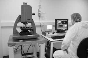
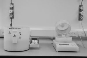
Jacomex Glovebox
The Jacomex GP (Campus) is a 4 gloves glovebox for both 2D materials identification and fabrication and characterization. Its Argon atmosphere, low Oxygen (<1ppm) and water (<2ppm) levels makes it ideal for exfoliation and manipulation of 2D materials, ensuring them to remain pristine and non-oxidised. It includes a home-built transfer setup for accurate positioning (within 1um accuracy) and stacking of 2D materials. A home-built optical microscope in reflection allows thickness identification via contrast method, capable of fluorescence analysis for a fast and reliable 2D-semiconductor single layer determination. The integration of the EP4 nanofilm ellipsometer within the glovebox opens up the possibility for automated flakesearch, and ellipsometry measurements, with the addition of an atomic force microscope (nanosurf FlexAFM) with piezoresponse capabilities (PFM) for an accurate moiré superlattice visualization in twisted 2D devices.
Heidelberg DWL 66+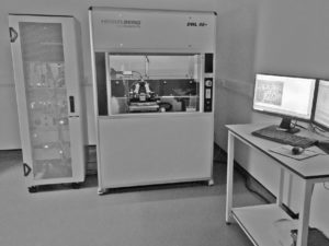
The Heidelberg DWL 66+ is a laser lithography machine for both mask making and direct photo-resist patterning. Substrates of up to 200 x 200 mm2 and structures down to 300 nm can be made using this system. Two CCD cameras enable the system to perform overlay exposures with high accuracy. It is also possible to crease 3D structures using the Advanced Gray Scale Exposure Mode.
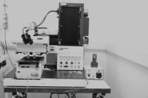
Accurion Nanofilm EP4 Imaging Ellipsometer
This new microscopic thin film, surface and materials metrology tool generation uses a combination of ellipsometry and microscopy to enable surface characterization with a lateral ellipsometric resolution down to 1 micron. It can accurately measure film thicknesses and refractive indexes even in multi-layer coatings. The nanofilm_ep4 has sophisticated modelling software. Separate modules simplify the instrument operation enabling parallel or offline analysis of collected data remote from the instrument.
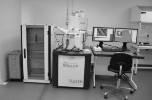
Raith Pioneer Electron Beam Lithography
The Raith PIONEER combines ultra-high resolution electron beam lithography (EBL) and scanning electron microscopy (SEM). The PIONEER features 30kV column technology and an accurate laser controlled stage.
The Leica SEM platform is a high quality instrument with both SE and inlens detectors ensuring high quality images. Integral software allows designs to be created, edited and written in one session making this an ideal multi-purpose instrument.
Applications for this instrument include Nanolithography, SEM imaging, Material and structural analysis, Chip scanning.
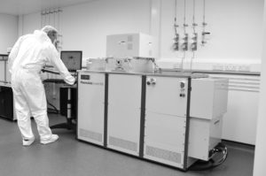 Plasmalab System 100 Reactive Ion Etch Machine with ICP
RIE is a type of dry etching with different characteristics from a wet etch. RIE uses chemically reactive plasma to remove material deposited on wafers and is used extensively in microfabrication.
The Oxford Plasmalab System 100 is a 100 mm reactive ion etching tool and with a wide range of gases available and recipes to etch many materials, it is an invaluable piece of equipment in the lab. The tool uses a simple program on a windows operating system to run recipes and it’s very intuitive and easy to learn and use. The ICP facility allows deep etching of Silicon to around 20µm depth depending on the mask material. This is an excellent partner tool for the Pioneer Electron Beam Lithography as well as the optical lithography equipment.
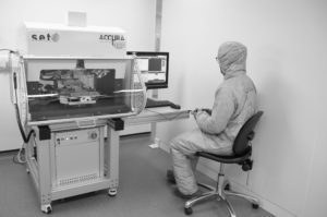
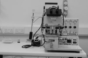
SET ACCμRA 100 High Accuracy Flip Chip Bonder
The ACCµRA 100 is an Education and R&D oriented flip-chip bonder that allows ± 0.5 µm accuracy. Motorized axes guarantee a high repeatability of your process and its flexibility makes it ideal for developing a wide range of applications. ACCµRA 100 combines high precision, accessibility and cost-effectiveness. It is the perfect equipment for universities and R&D institutes.
Applications include…
- Micro assembly
- Laser diode, laser bar
- VCSEL, photo diode
- LED
- Flip-chip bonding, die bonding
- Chip-to-chip, chip-to-substrate bonding
- MOEMS, MEMS, MCM packaging…
- 3D packaging
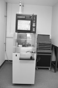
Disco DAD3220 Wafer Dicing Saw
The DAD3220 is a single spindle dicing saw capable of handling workpieces up to a maximum of ø6" or 6" square. It is ideal for processing electronic component materials such as glasses and ceramics. It is designed for high precision and process quality for cutting and grooving optical components, magnetic heads, and similar workpieces with extremely strict tolerances.
It has auto-alignment, auto-focus, and autokerf check functions for enhanced productivity and is a suitable tool for small production runs as well as R&D quantities.
Contact Lithography Equipment
Karl Suss Mask Aligners, both an MJB3 and an MA6 are extensively used in the lab for contact lithography and two spin coaters are available for preparing substrates with a range of available photoresists.
Photomasks can be provided by an external source but can now be produced in-house with the Heidelberg laser lithography system
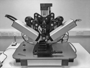
Nanosurf FlexAFM with PFM capabilities
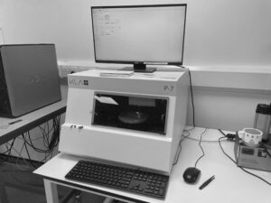
Profilometer KLA+ P-7
Zygo Optical Test Interferometer